


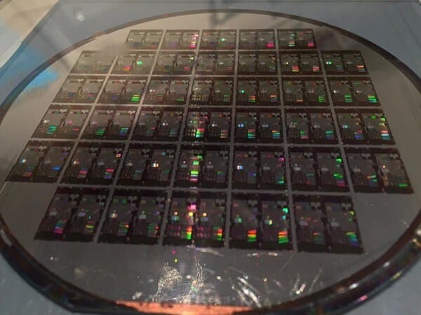
A recent study published in the IEEE Journal of Lightwave Technology reveals a significant breakthrough in photonic integration, as researchers from the University of California successfully demonstrated the monolithic integration of indium arsenide quantum dot (QD) lasers onto silicon chiplets.
Led by Dr. Rosalyn Koscica, the team overcame longstanding material mismatch challenges between III-V semiconductors and silicon—a key barrier to embedding efficient laser sources directly on photonic chips. “Photonic integrated circuit applications call for on-chip light sources with a small device footprint to permit denser component integration,” said Dr. Koscica.
To achieve the integration, the researchers employed a three-part strategy: the pocket laser concept for monolithic assembly, a two-step material growth method combining metalorganic chemical vapor deposition (MOCVD) and molecular beam epitaxy (MBE), and a polymer gap-fill technique to reduce beam divergence and improve coupling efficiency.
The resulting silicon chiplets with integrated QD lasers exhibited low coupling loss and efficient lasing at a single O-band wavelength—ideal for low-dispersion signal transmission in photonic devices. Frequency selectivity was achieved using silicon-based ring resonators or silicon nitride-based distributed Bragg reflectors.
Importantly, the QD lasers maintained stable lasing at temperatures as high as 105°C and demonstrated an estimated lifespan of 6.2 years at 35°C operating conditions—indicating reliability for long-term deployment.
The integration method is scalable and compatible with a wide range of photonic circuit architectures, offering a promising path toward compact, cost-effective light sources for data centers, telecommunications, and sensing applications. The findings mark a critical step toward practical, scalable silicon photonics with embedded laser functionality.