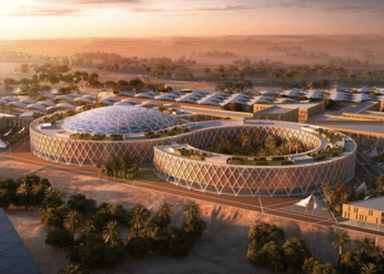

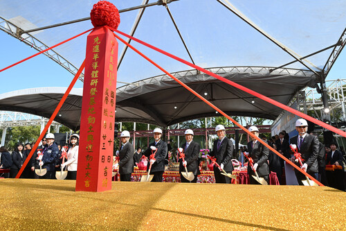
The Advanced Semiconductor R&D Center has officially broken ground at the headquarters campus of the Industrial Technology Research Institute (ITRI) in Hsinchu, signaling a new phase in Taiwan’s strategy to reinforce its position in the global semiconductor value chain.
The project is being jointly developed by the Ministry of Economic Affairs, National Development Council, and National Science and Technology Council. Officials said the center is designed to reduce verification barriers for small and mid-sized integrated circuit (IC) design firms and startups, helping bridge the gap between laboratory research and large-scale industrial commercialization.
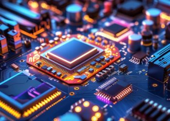
Scheduled for completion by the end of 2027, the facility will integrate three primary functions: innovative IC design verification, advanced process development, and localized validation of equipment and materials. It will house Taiwan’s first 12-inch advanced pilot line established by a research institution, alongside upgraded 8-inch facilities. The combined infrastructure is intended to create a seamless environment connecting chip design, fabrication, packaging, and testing.
Minister of Economic Affairs Kung Ming-hsin noted that Taiwan recorded 8.36% economic growth last year, driven largely by the semiconductor and artificial intelligence sectors. He emphasized the ministry’s continued support for SMEs through diversified, small-scale chip prototyping initiatives. The new center, he said, will operate as a one-stop service platform, enabling companies to conduct design verification, manufacturing trials, and packaging and testing in a consolidated setting.
In addition to supporting IC design firms, the center will provide materials and equipment suppliers with on-site demonstration and validation opportunities, potentially accelerating their integration into global supply chains.
The facility is expected to offer 28–90 nm back-end-of-line process R&D and pilot production services, with a goal of shortening product development cycles by approximately 30%. It will support emerging applications including AI chips, silicon photonics, quantum technologies, ASICs, 3D integration, and next-generation memory.
Officials say the center is part of a broader effort to build a resilient, self-reliant semiconductor innovation ecosystem, strengthen academic collaboration, and expand Taiwan’s semiconductor talent pipeline.