

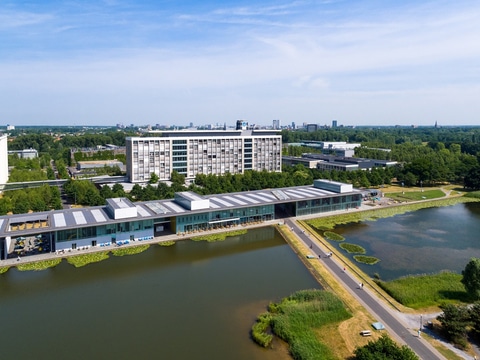
Dai Nippon Printing Co., Ltd. (DNP) (TOKYO: 7912) announced plans to open its first overseas research and development center in Eindhoven, the Netherlands, in September 2025. The facility will be located within the High Tech Campus Eindhoven (HTCE), a major European innovation hub home to over 300 tech companies and more than 12,500 researchers and engineers.
The move marks a strategic expansion by DNP to globalize its R&D efforts and accelerate innovation in advanced semiconductor packaging technologies. The new center’s initial focus will be on Co-Packaged Optics, a next-generation technology that integrates optical and electronic components to enhance data processing performance while reducing energy consumption.
In tandem with the center’s launch, DNP has entered into a joint research agreement with the Netherlands Organization for Applied Scientific Research (TNO), announced in July. The collaboration will involve the Photonic Integration Technology Centre (PITC), also located at HTCE, which specializes in transitioning photonic chip research to scalable production.
Over a planned three-year research timeline, DNP aims to develop package components using precision patterning technologies for optical materials and to foster partnerships across HTCE’s research ecosystem.
The company sees the Netherlands facility as a gateway to advanced technologies and collaborative networks in the field of photonics and semiconductor packaging. The initiative supports DNP’s broader goals of energy-efficient, high-performance product development for the next wave of computing demands.
Founded in 1876, DNP has evolved from a traditional printing company into a diversified technology leader across fields including display components, packaging, and electronics.