


CDimension, a next-generation semiconductor startup founded by MIT alumni, has launched the commercial availability of its ultra-thin 2D materials—marking a pivotal milestone in its mission to fundamentally reimagine computing hardware. The debut moves the company from lab innovation to real-world deployment, setting the stage for a radical shift in how chips are designed and built.
The company’s proprietary low-temperature process enables the direct growth of 2D semiconductor materials—such as molybdenum disulfide (MoS₂)—on fully fabricated silicon wafers without damaging underlying circuitry. This process is compatible with standard back-end-of-line (BEOL) silicon manufacturing, overcoming one of the major barriers that has long limited the commercial adoption of 2D materials in semiconductors.
“Our computational systems are breaking under the weight of increasing demand,” said Jiadi Zhu, founder and CEO of CDimension and an MIT Ph.D. in electrical engineering. “We’ve reached a point where traditional architectures and materials can no longer keep up. CDimension is focused on solving this problem at the root—by rethinking the physical building blocks of modern chips.”
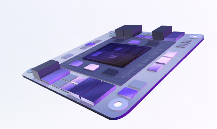
CDimension’s 2D materials platform is designed to support vertically stacked, energy-efficient architectures that unify compute, memory, and power in a single chip. Targeted at high-growth sectors such as AI, robotics, quantum computing, and edge workloads, the materials offer dramatic performance improvements: up to 1,000× better transistor-level energy efficiency compared to silicon, with a broader roadmap including 100× system-level energy gains, 100× greater integration density, and 10× faster operating frequencies through reduced parasitic losses.
These performance gains are enabled by the atomic thinness and electrical properties of the company’s 2D materials, which support dense vertical stacking and low-leakage operation. The materials are now available for commercial sampling and integration at research-accessible pricing, and are already being evaluated by early partners across academia and industry.
“2D materials have long held promise for the semiconductor industry, but the leap from research to manufacturing has been elusive,” said Dr. Jing Kong, MIT professor and renowned expert in 2D material synthesis. “CDimension’s BEOL-compatible, wafer-scale growth technique represents a breakthrough moment—one that can unlock entirely new architectures for memory, power, and compute.”
CDimension’s initial materials portfolio includes n-type, p-type, metallic, and insulating films—produced through a wafer-scale deposition process that aligns with existing semiconductor workflows. By offering a full material stack, the company positions itself not just as a materials supplier, but as a hardware platform enabler.
As silicon-based chip architectures hit physical and economic limits, the industry faces rising challenges: thermal bottlenecks, soaring energy costs, and fragmented chiplet packaging that impedes performance. CDimension’s approach to monolithic 3D integration—stacking atomically thin chiplets directly atop one another—eliminates interconnect delays and drastically improves system-level performance and efficiency.
“AI models are doubling in size every few months, and yet we’re still running them on 20th-century architecture,” said Zhu. “The only way forward is a radical overhaul—starting not with the software, but with the atoms that form our chips.”
To support R&D and adoption, CDimension has launched a Premier Membership Program offering custom services including monolayer deposition over 3D structures and growth on up to 12-inch arbitrary wafers. These services enable researchers and early adopters to build, test, and prototype 2D-material-based circuits and architectures.
The company, guided by Zhu’s research at MIT under Professor Tomás Palacios—Director of the Microsystems Technology Laboratories—holds multiple patents across materials synthesis, process integration, and chip architecture. CDimension’s technology roadmap points toward a unified computing architecture capable of delivering unprecedented energy efficiency and computational density.
While the commercial release of 2D materials is the company’s first public milestone, it signals a much broader ambition: to rebuild the computing stack from the ground up. The company’s end goal is a fully vertically integrated chip that merges logic, memory, and power delivery into one cohesive, high-performance system.
“In a world of exponentially growing data and AI complexity, we need hardware that evolves just as fast,” Zhu said. “This launch is just the beginning of that future.”