


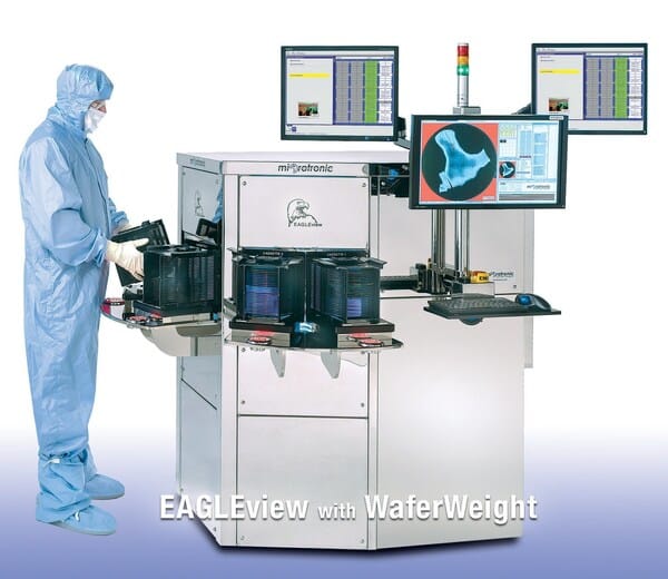
Microtronic, a semiconductor inspection technology company founded in 1994 and headquartered in Hawthorne, New York, has announced the launch of WaferWeight, a patented solution designed to precisely monitor wafer mass during macro defect inspection. The technology is fully integrated into the company’s EAGLEview line of high-speed inspection systems and is available for both the latest EAGLEview 6 model and earlier generations.
As semiconductor manufacturing processes continue to evolve in complexity, precise tracking of wafer mass changes has become increasingly essential for effective process control. WaferWeight addresses this need by allowing fabs to monitor wafer weight variations concurrently with defect inspection, eliminating the need for separate metrology tools.
“Wafer mass metrology is gaining importance as devices become more sensitive to minute process variations,” said Reiner Fenske, CEO of Microtronic. “WaferWeight provides fabs with an efficient, high-precision method to detect subtle mass changes at key stages—such as deposition, etch, plating, backgrinding, bonding, and TSV—without impacting throughput.”
The system offers measurement resolution as low as 0.1 milligrams, enabling accurate detection of mass fluctuations across wafers and processing steps. These variations—often undetectable by visual inspection—can be critical indicators of underlying process deviations. High-throughput capability, a hallmark of the EAGLEview platform, allows for comprehensive wafer-by-wafer data collection, ensuring tight statistical process control (SPC) in high-volume manufacturing environments.
Captured data is managed through Microtronic’s ProcessGuard software, which logs wafer information by lot, time, and slot position. The software’s integrated Slot-Positional Analysis Tool provides detailed insight into weight trends and pre/post-process deltas, helping fabs improve traceability, yield, and operational efficiency.
With the introduction of WaferWeight, Microtronic strengthens its role in delivering integrated, scalable solutions for semiconductor manufacturing.