


Cadence Design Systems Inc. (Nasdaq: CDNS) has announced the tapeout of the industry’s first LPDDR6/5X memory IP system optimized for 14.4Gbps data rates, marking a significant leap in memory performance aimed at powering next-generation AI infrastructure. The new offering, up to 50% faster than previous LPDDR memory standards, is designed to meet the escalating bandwidth and capacity requirements of advanced AI applications, including large language models (LLMs), agentic AI systems, and compute-heavy workloads in high-performance computing (HPC) and data centers.
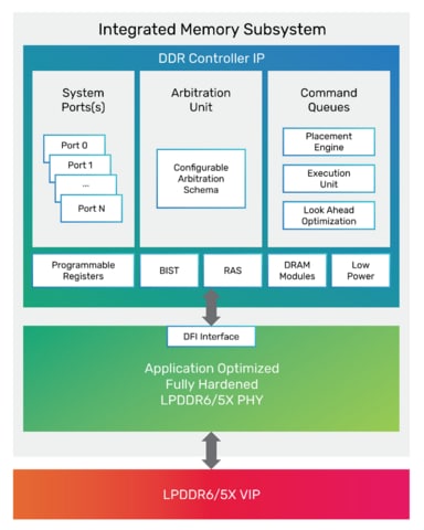
Cadence’s new memory IP supports the JEDEC LPDDR6/5X standards and combines a high-performance controller with a new PHY architecture to deliver optimal power, performance, and area (PPA) metrics. The solution is engineered for integration into both traditional monolithic system-on-chips (SoCs) and multi-die architectures, leveraging Cadence’s chiplet framework to facilitate heterogeneous integration.
“The evolution of data centers from high-performance compute to AI training and inference at scale has created unprecedented demand for efficient memory bandwidth,” said Boyd Phelps, senior vice president and general manager of the Silicon Solutions Group at Cadence. “LPDDR6 has emerged as a key enabler for accelerated compute. With this tapeout, Cadence extends its leadership in memory IP by offering a highly integrated LPDDR6 system solution tailored to customer-specific requirements.”
The LPDDR6/5X memory IP system is built on Cadence’s experience with previous high-speed memory standards, including DDR5 (12.8Gbps), LPDDR5X (10.7Gbps), and GDDR7 (up to 36Gbps). The latest product supports LPDDR6, LPDDR5X, and LPDDR5X CAMM2, offering flexibility for AI, mobile, enterprise, and cloud markets.
Cadence has already engaged with several leading AI and HPC customers to implement the new solution. The PHY component is customizable for varied package and system topologies and is available as a hardened macro for rapid deployment. The memory controller, delivered as a soft RTL macro, supports the Arm AMBA AXI interface and offers a full suite of standard and advanced features for scalable performance and power efficiency.
As part of its broader ecosystem offering, Cadence also provides a complete LPDDR6 Memory Model, allowing SoC designers to verify protocol compliance, perform functional coverage, and accelerate development cycles with greater confidence.
The new memory IP joins Cadence’s comprehensive memory system portfolio, which includes DDR, GDDR, and HBM solutions. Designed using Cadence’s leading analog/mixed-signal tools and integrated with its UCIe-based chiplet framework, the LPDDR6/5X IP provides a foundation for rapid chiplet-based product realization—supporting a growing need for scalable, high-performance compute platforms across AI and data-intensive applications.
The LPDDR6/5X memory IP is now available for customer engagements.